
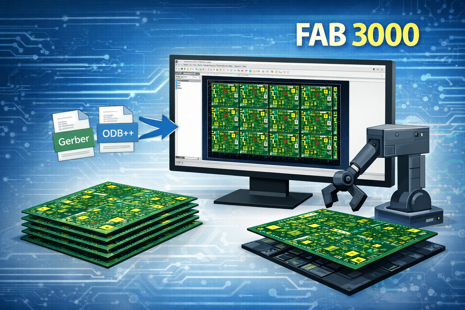
How to Create PCB Panels in FAB 3000 (Step-by-Step Guide)
PCB panelization is one of the most effective ways to improve manufacturing efficiency, reduce production costs, and streamline your workflow.
Instead of processing one board at a time, panelization allows you to combine multiple PCB designs into a single panel—making fabrication and assembly faster, more consistent, and more cost-effective.
With FAB 3000, creating PCB panels is fast, flexible, and incredibly powerful—even if you're working with just Gerber or ODB++ files.
🎬 Watch the full panelization workflow in FAB 3000:
Prefer a quick walkthrough? Watch the video above.
Want step-by-step details? Follow the guide below.
What Is PCB Panelization (And Why It Matters)
PCB panelization is the process of grouping multiple circuit boards into a single manufacturing panel.
This allows you to:
- Process multiple boards at once
- Reduce material waste
- Improve assembly efficiency
- Minimize handling errors
Think of it like running a full production batch instead of one unit at a time—it's faster, more efficient, and more scalable.
Why Use FAB 3000 for Panelization
FAB 3000 gives you complete control over your panel layout—even without original design files.
With FAB 3000, you can:
- Create panels with unlimited PCB copies
- Work with Gerber, ODB++, and other formats
- Build mixed "family panels" with different designs
- Modify layouts without going back to CAD
- Export clean, production-ready files
Step-by-Step: Panelization Workflow in FAB 3000
1. Import Your PCB Data
Start by loading your files into FAB 3000 (Gerber, ODB++, etc.). Ensure all layers are aligned correctly.
2. Save Your Design as a Job File
Save your PCB as a job file so it can be reused and inserted multiple times into a panel.
3. Create a New Panel Layout
Define panel size, spacing, and layout orientation.
4. Step-and-Repeat Your Design
Duplicate your PCB across the panel to maximize efficiency and throughput.
5. Create Mixed (Family) Panels
Combine multiple PCB designs into one panel for prototyping or low-volume production.
6. Adjust Layout and Spacing
Refine spacing, alignment, and edge clearance for proper manufacturing handling.
7. Export Your Panel
Export your final panel in Gerber, ODB++, or DXF format for production.
Panelization Methods to Consider
- V-Scoring – best for straight-line separation
- Tab Routing – ideal for complex board shapes
Real-World Benefits of Panelization
- Reduce manufacturing costs
- Speed up assembly
- Improve consistency
- Minimize handling damage
Final Thoughts
Panelization is one of the most valuable skills in PCB manufacturing—and with FAB 3000, it's easier than ever to implement.
Whether you're working with Gerber files, ODB++ data, or reverse-engineering designs, FAB 3000 gives you the tools to build panels quickly, customize layouts, and produce manufacturing-ready outputs with confidence.
Get Started with FAB 3000 Today
Ready to start creating PCB panels faster and more efficiently? With FAB 3000, you can streamline your panelization workflow, reduce errors, and produce clean, manufacturing-ready outputs—all without needing the original design files.
Take control of your CAM workflow—and become the go-to expert for PCB panelization.