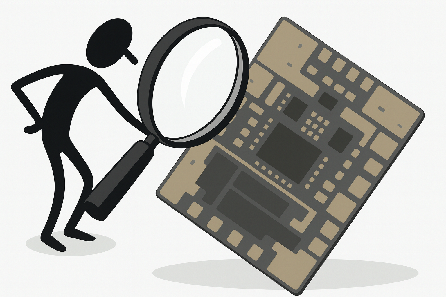
Advanced DFM Checks for PCB Manufacturing | FAB 3000
Most PCB layout software will display your PCB design perfectly on the screen, and pass it through their Design Rules Check (DRC) with 'flying colors'. At this point you should be confident enough to generate Gerber/NC files and send them out for fabrication... Right?
Unfortunately Wrong...
There are two common mistakes which may cause your boards to fail and become very costly to your wallet and reputation:
1.Don't Automatically Trust Your Gerber Files
PCB layout software has always had a history of not being able to output "100% reliable" Gerber files (plane layers especially).
Why is there a problem outputting reliable Gerber files? The Gerber Format is just unintelligent X,Y coordinate data with apertures (that's right apertures which were used in early plotters back in the 70's). To output Gerber files, your PCB layout software must dismantle and break apart its' own intelligent design database - down to simple X,Y coordinates and apertures. Generating Gerber files for plane layers (power/ground) and mixed technology are the most prone to hidden problems and mistakes.
What about ODB++ and IPC-2581, will these new formats eliminate the problem? Unfortunately no, the same problem still exists when outputting to other manufacturing formats such as ODB++, IPC-2581, etc. These formats are more advanced but still built upon a foundation which uses X,Y coordinates with shapes (i.e Apertures). The same mistakes that appear in Gerber commonly appear in these newer formats.
Important: It really doesn't matter what your PCB layout software displays on the screen or the results from their DRC checks... it's the outputted gerber files which determine the final quality of your boards. Here's a more detailed article about these potential pitfalls: Don't blindly trust your Gerbers
2.Lack of True Manufacturing Checks (DFM)
A PCB layout software's primary focus is to check for design integrity and not necessarily manufacturing integrity.
Manufacturing specific issues are much more difficult to detect and can quietly cause your boards to fail or have poor performance. Common manufacturing checks (DFM) include: Acid traps, Copper Slivers, Antennas, Solder Bridging, Starved Thermal, Ground Plane Check, Thermal Conflicts and much more.
An Independent Third Party DFM Check is Essential: Avoid using DFM software and PCB Layout software created by the same company. Chances are if their PCB Layout software missed a manufacturing problem, those same mistakes will get overlooked or unnoticed in their DFM software. An independent third party DFM solution is always recommended for the most reliable results.
Advanced DFM Check Sections
DFM Check Severity Levels
The PCB will fail and/or have very low manufacturing yields.
May result in poor PCB performance.
Cause delays and/or additional problems during PCB fabrication.
Signal DFM Checks
Acid Traps
Due to the surface tension during the etching process, larger deposits of acid may get trapped into certain areas - resulting in over-etching.
Critical: Over-etching will directly effect your board yields and performance.
Find Net Discrepancy
Search for overlapping copper objects which have different nets defined. This net discrepancy typically occurs when the PCB layout software has incorrectly outputted intelligent formats such as ODB++ and IPC-2581.
Critical: Indicates a potential short originating from the PCB design. May result in poor board performance, failure, or other undesired effects.
Copper Slivers
Narrow areas in the copper where the potential for over-etching is great. This typically happens when trace angles are 30 degrees (or less), when composites are used, and on plane layers.
Critical: A board can fail if certain copper area are over-etched. Resulting in shorts and decrease in board yield.
Antennas / Dangling Traces
Search for Non-terminating traces which may behave as an antenna. Such traces may be intentional, but a warning is reported as a precaution.
Elevated Risk: May result in poor board performance, short, or other undesired effect.
Minimum Clearance: Outer Layers
May cause under-etching on copper areas and/or exceed PCB fabricators capabilities. Resulting in possible opens or shorts.
Critical: May result in poor board performance, short, or other undesired effect.
Minimum Clearance: Inner Layers
May cause under-etching on copper areas and/or exceed PCB fabricators capabilities. Resulting in possible opens or shorts.
Critical: May result in poor board performance, short, or other undesired effect.
Minimum Annular Ring: Drill-Pad
Search for all plated drills and ensure they have a minimum copper annular ring. Having a minimum copper annular ring around each drilled hole is required to assure it will be properly fabricated.
Critical: In many cases, drilled holes are not perfectly registered within the exact center of each copper pad. Not having enough of a copper annular ring, may make plating on vias, as well as solder-ability on component holes more difficult. In extreme cases, may result in poor board performance, failure, or other undesired effects.
Minimum Clearance: Track-Track
Locate tracks (with different nets) on the same signal layer that are placed too close to each other.
Critical: May cause under-etching on copper areas and/or exceed PCB fabricators capabilities. Resulting in poor board performance, short, or other undesired effects.
Minimum Clearance: Track-Pad
Locate tracks and pads (with different nets) on the same signal layer that are placed too close to each other.
Critical: May cause under-etching on copper areas and/or exceed PCB fabricators capabilities. Resulting in possible opens, shorts, or other undesired effects.
Minimum Clearance: Pad-Pad
A copper pad on the signal layer is placed too close to other copper pads (with a different net).
Critical: May cause under-etching on copper areas and/or exceed PCB fabricators capabilities. Resulting in possible opens, shorts, or other undesired effects.
Non-Functional Internal Pads
Essentially these are unconnected internal pads typically found on plane layers.
Elevated Risk: May break loose and cause potential drilling problems, risk of shorts, and more.
Minimum Pad Size
A very small diameter pad placed on a signal layer. This typically occurs when incorrect pad stacks are defined within the PCB layout software, or an error has occurred when PCB layout software has generated the Gerber data.
Elevated Risk: May cause etching or soldering problems during fabrication. Smaller pads also provide less mechanical support for component leads.
Clearance from Board Edge
Objects are placed too close or outside the PCB border.
Elevated Risk: May result in exposed copper at the board edge which could lead to corrosion and long term reliability problems.
Minimum Width: SMT Pad
Locate SMT pads on top/bottom signal layers that have a smaller width than permitted.
Elevated Risk: May cause under-etching and/or uneven pad widths. May also result in poor soldering performance & misalignment during assembly.
Minimum Clearance: Rout-Copper
Search for Rout paths that are too close to signal objects.
Elevated Risk: During NC routing process, copper may be damaged or result in other undesired effects.
Minimum Clearance: Same Net
Locate objects on the same net and signal layer that are too close to each other.
Elevated Risk: May cause under-etching on copper areas and/or exceed PCB fabricators capabilities. Resulting in possible opens or shorts.
Hole Registration
Find drill holes that do no align with copper pads, due to potential rounding errors found in the drill data, or other causes.
Elevated Risk: This may make plating on vias, as well as solder-ability on component holes more difficult. In extreme cases, may result in poor board performance, failure, or other undesired effects.
Redundant Pads
Duplicate pads are commonly included in the manufacturing data generated from PCB layout software.
Common: This duplication may result in bloated file sizes, potential issues during DFM verification, NC drilling, and your wallet. That's correct your wallet. Many PCB fabricators use pad counts and drill counts as a factor when quoting prices to manufacture a PCB. Having excessive pad and/or drill counts could lead to increased manufacturing costs.
Minimum Width: Track
Locate tracks which have a smaller width than the allocated distance.
Common: May cause etching problems during fabrication. The smaller the trace width, the lower the yield for the PCB fabricator and the more costly your boards may be.
Plane DFM Checks
Power/Ground Short
Determine any potential shorts between Power and Ground planes.
Critical: A board will fail if there is a short between the power and ground planes.
Starved Thermal
Check whether a thermal connection to the copper plane has been constricted by overlapping or adjacent data that is way too close.
Elevated Risk: May result in poor board performance, short, or other undesired effect.
Neg. Plane Thermal Conflicts
Determine if any via or plated hole is connected to more than one negative plane together.
Elevated Risk: May result in poor board performance.
Isolated Connections
One of the most common problems is to determine whether your PCB CAD system has properly outputted good plane connections to the copper plane.
Critical: A board will fail if any plane connections is not properly connect the copper plane.
Drill Registration
Locate any plated drill holes that do not center over an existing pad. Most likely the Drill layer has either been generated or imported incorrectly.
Elevated Risk: This will lead to problems during PCB fabrication.
Minimum Annular Ring: Drill-Plane
Search for all plated drills on plane (GND/VDD) layers and ensure they have a minimum copper annular ring. Having a minimum copper annular ring around each drilled hole is required to assure it will be properly fabricated.
Critical: In many cases, drilled holes are not perfectly registered within the exact center of each pad. Not having enough of an annular ring, may result in poor board performance, failure, or other undesired effects.
Minimum Clearance: Plane
May cause under-etching on copper areas and/or exceed PCB fabricators capabilities. Resulting in possible opens or shorts.
Critical: May result in poor board performance, short, or other undesired effect.
Minimum Width: Plane
Locate metal areas on the plane which have a smaller width than the allocated distance. This typically occurs when PCB layout software has incorrectly generated complex polygons with holes (i.e. dark/clear areas) for the plane layers in the Gerber data.
Elevated Risk: May result in poor board performance, short, or other undesired effect.
Minimum Thermal Air gap
The minimum gap permitted between the edge of a thermal connect pad and copper area.
Elevated Risk: May result in poor board performance, short, or other undesired effect.
Minimum Thermal Spoke Width
The minimum allowable width for a thermal spoke.
Elevated Risk: May result in poor board performance, short, or other undesired effect.
Minimum Clearance: Plane to Drill
Search for all plated drills and ensure they have a minimum clearance from the plane. Having a minimum spacing around each drilled hole is required to assure there will be no shorts or other undesired affects.
Elevated Risk: In many cases, drilled holes are not perfectly registered within the exact center of each clearance pad. Not having enough of a clearance, may result in poor board performance, failure, or other undesired effects.
Minimum Clearance: Plane to Rout
Search for Rout paths that are too close to plane objects.
Elevated Risk: During NC routing process, copper may be damaged or result in other undesired effects.
Silkscreen DFM Checks
Minimum Clearance: Silk Screen to Board Edge
The minimum clearance allowed from Silkscreen to board edge. Any silkscreen objects outside the board edge will also be flagged.
Elevated Risk: This will lead to problems during PCB fabrication.
Minimum Width: Silkscreen Line
Check for the minimum width for each object on the silkscreen.
Common: If the line width is too thin it will not be legible on the fabricated PCB.
Minimum Silkscreen Text Height
Determine whether the Text height is large enough on the silkscreen layers.
Common: If the text height is too small it will not be legible on the fabricated PCB.
Silkscreen over Solder Mask
Locate if there are any areas where the silkscreen overlaps with openings in the solder mask layers.
Elevated Risk: May cause contamination of the pads and make electrical testing plus SMT soldering more difficult.
Minimum Clearance: Silk Screen to Copper
Verify the minimum clearance between silkscreen objects and copper objects (performed on top and bottom signal layers only).
Elevated Risk: May cause contamination of the pads and lead to problems during PCB fabrication.
Minimum Clearance: Silk Screen to Drill
Verify the minimum clearance between silkscreen objects and drilled holes (both plated and unplated).
Common: May cause problems during PCB fabrication.
Minimum Clearance: Silk Screen to Rout
Verify the minimum clearance between silkscreen objects and routed paths.
Common: May cause problems during PCB fabrication.
Minimum Clearance: Silk Screen (Line to Line)
Verify the minimum clearance between silkscreen line objects.
Common: May cause problems during PCB fabrication.
Minimum Clearance: Silk Screen (Line to Pad)
Verify the minimum clearance between silkscreen line and pad objects.
Common: May cause problems during PCB fabrication.
Minimum Clearance: Silk Screen (Pad to Pad)
Verify the minimum clearance between silkscreen pad objects.
Common: May cause problems during PCB fabrication.
Solder Mask DFM Checks
Mask Slivers
Areas in the solder mask where the resist is so narrow that it may cause small pieces of the resist to flake off and present soldering problems later.
Critical: A board can fail if the resist lifts in an area that needs to be soldered later on.
Solder Bridges
Typically when the mask layers, contain openings which are too large, and may expose other adjacent conductive areas.
Critical: During fabrication, copper may get too close and form a bridge to other adjacent conductive areas.
Undersized Mask Clearances
Used to locate mask openings that may cause de-lamination from the PCB substrate.
Missing Mask Clearances
Locate areas where mask clearances are missing.
Minimum Clearance: Solder Mask to Rout
Check minimum clearance between solder mask and routed paths.
Common: May cause problems during PCB fabrication.
Minimum Clearance: Mask (Draw to Draw)
Verify minimum clearance between solder mask draw objects.
Common: May cause problems during PCB fabrication.
Minimum Clearance: Mask (Draw to Pad)
Verify minimum clearance between solder mask draw and pad objects.
Common: May cause problems during PCB fabrication.
Minimum Clearance: Mask (Pad to Pad)
Verify minimum clearance between solder mask pad objects.
Common: May cause problems during PCB fabrication.
Partial Clearances
Locate partial mask clearances that may cause issues.
Common: May cause problems during PCB fabrication.
Drill DFM Checks
Drill-Plane Shorts
Detect potential shorts between drill holes and plane layers.
Minimum Drill Size
Verify that all drill holes meet the minimum size requirements.
Double Drill Hits
Duplicate drill hits are commonly included in the manufacturing data generated from PCB layout software.
Common: This duplication may result in potential issues during DFM verification, blowouts during NC drilling, and your wallet. That's correct your wallet. Many PCB fabricators use drill counts as a factor when quoting prices to manufacture a PCB. Having excessive drill counts could lead to increased manufacturing costs.
Pads without Drills
Locate pads that should have drill holes but don't.
Common: May cause problems during PCB fabrication.
Plated Drill without Pads
Search for all plated drills and ensure they have a minimum copper annular ring on all required metal layers. Having a minimum copper annular ring around each drilled hole is required to assure it will be properly fabricated.
Elevated Risk: In many cases, drilled holes are not perfectly registered within the exact center of each copper pad. Not having enough of a copper annular ring, may make plating on vias, as well as solder-ability on component holes more difficult.
Touching Drill Hits
Occurs when drilled holes are placed too close to other drilled holes on the circuit board.
Common: When trying to drill holes that are too close together, it may cause the drill bits to break during the drilling process. This effect is also known as blowouts.
Minimum Clearance: Plated Drills to Copper
Verify minimum clearance between plated drills and copper areas.
Common: May cause problems during PCB fabrication.
Minimum Clearance: Unplated Drills to Copper
Verify minimum clearance between unplated drills and copper areas.
Common: May cause problems during PCB fabrication.
Minimum Clearance: Drills to Rout
Check minimum clearance between drills and routed paths.
Common: May cause problems during PCB fabrication.
Minimum Clearance: Rout to Rout
Verify minimum clearance between routed paths.
Common: May cause problems during PCB fabrication.
Minimum Drill Hole Spacing
Ensure adequate spacing between drill holes.
Common: May cause problems during PCB fabrication.
Assembly DFM Checks
Minimum Clearance: Component
Verify spacing between components is greater than the minimum permitted value. The component outline is determined by either (1) the extent of its pins and any geometric objects drawn in silkscreen, or (2) The extents provided when importing an intelligent ODB++ or IPC-2581 file.
Critical: Components that are placed too close together may prevent the board from properly being assembled.
Maximum Component Height
Check each component height and determine if it exceeds the maximum permitted value.
Elevated Risk: If a component exceeds the maximum permitted height it may prevent a fully assembled PCB from properly fitting into a designed enclosure.
Component Overlaps
Verify components do not intersect. The component outline is determined by either (1) the extent of its pins and any geometric objects drawn in silkscreen, or (2) The extents provided when importing an intelligent ODB++ or IPC-2581 file.
Critical: Components that overlap will prevent the board from properly being assembled.
Invalid RefDes
Detect invalid or missing reference designators on components.
Invalid Component Rotation
Check for components with incorrect rotation angles.
Footprint to Pad Registration
Verify that component footprints align properly with pad locations.
SMT Stencil DFM Checks
Minimum Width: SMT Stencil Pad
Locate SMT pads on top/bottom paste layers that have a smaller width than permitted.
Elevated Risk: May cause under-etching and/or uneven pad widths during SMT stencil fabrication. May also result in poor soldering performance & misalignment during assembly.
Minimum Aspect Ratio: SMT Stencil Pad
Locate SMT pads on top/bottom paste layers that have a smaller Aspect Ratio than permitted. The Aspect ratio equals the paste pad width divided by the stencil foil thickness.
Elevated Risk: May cause under-etching and/or uneven pad widths during SMT stencil fabrication. May also result in poor soldering performance & misalignment during assembly.
Minimum Area Ratio: SMT Stencil Pad
Locate SMT pads on top/bottom paste layers that have a smaller Area Ratio than permitted. The Area ratio equals the paste pad area divided by the paste pad height and stencil foil thickness.
Elevated Risk: May cause under-etching and/or uneven pad widths during SMT stencil fabrication. May also result in poor soldering performance & misalignment during assembly.
Minimum Volume: SMT Stencil Pad
Locate SMT pads on top/bottom paste layers that have a smaller paste volume than permitted. The paste volume equals the paste pad area and stencil foil thickness.
Elevated Risk: Excessive paste volume may result in poor soldering performance & bridging during assembly.
SMT Stencil Pad to Pad Registration
Locate SMT pads on top/bottom paste layers and verify the align with pads located on top/bottom metal layers.
Elevated Risk: A SMT stencil pad misalignment (or registration issue) will cause problems during SMT stencil fabrication or pcb assembly.
Netlist DFM Checks
Open Net Detected
Check all test points and verify the same net is found at each defined location. A violation is highlighted if the extracted CAM net (which is generated from the manufacturing data) differs from the external net defined in the IPC Netlist file.
Critical: There is a very good chance your manufacturing data (Gerber, NC, ODB++, etc.) differs from your original PCB Design. A serious error has occurred either in your original PCB design or while exporting to your manufacturing data. A thorough review of your design in the highlighted areas is recommended. We also recommend you verify the export settings used while generating your manufacturing data.
Shorted Net Detected
Check all test points and verify the same net is found at each defined location. A violation is highlighted if the extracted CAM net (which is generated from the manufacturing data) connects with two or more different external nets defined in the IPC Netlist file. Essentially the same CAM net is found at two (or more) different external net locations.
Critical: There is a very good chance your manufacturing data (Gerber, NC, ODB++, etc.) differs from your original PCB Design. A serious error has occurred either in your original PCB design or while exporting to your manufacturing data. A thorough review of your design in the highlighted areas is recommended. We also recommend you verify the export settings used while generating your manufacturing data.
Missing Copper
Search each external net location (defined from the IPC Netlist file), and determine if an extracted CAM net (which is generated from the manufacturing data) exists.
Elevated Risk: Essentially an external net location was defined, but there was no CAM net found. This may be non-critical (caused by a single point net or CAM object without a net).
External Net Missing
An extracted CAM net (which is generated from the manufacturing data) exists where no external net was defined (from the IPC Netlist file).
Elevated Risk: Essentially a CAM net was detected without an external net defined. In many cases, this may not be considered a critical error.
Test Point DFM Checks
Minimum Test Point Diameter
Verify that all test points meet the minimum diameter requirements.
Common: May cause problems during PCB fabrication.
Minimum Distance: Test Point Center to Center
Ensure adequate spacing between test point centers.
Common: May cause problems during PCB fabrication.
Minimum Clearance: Test Point to Board Edge
Verify test points are placed at safe distance from board edge.
Common: May cause problems during PCB fabrication.
Minimum Clearance: Test Point Pad to Pad
Check clearance between test point pads.
Common: May cause problems during PCB fabrication.
Minimum Clearance: Test Point to Mask
Verify clearance between test points and solder mask.
Common: May cause problems during PCB fabrication.
Minimum Clearance: Test Point to Rout
Check clearance between test points and routed paths.
Common: May cause problems during PCB fabrication.
Find Test Point without Net
Locate test points that are not assigned to a net.
Common: May cause problems during PCB fabrication.
Run Professional DFM Checks Before You Fabricate
Don't risk production failures or expensive re-spins. FAB 3000 includes full advanced DFM analysis — including signal, plane, solder mask, silkscreen, netlist, drill, and assembly checks — so you can catch every issue before it reaches the manufacturer.
Download a Free Trial Today